Additive Manufacturing of Conductive Polymer Electronics
Additive manufacturing (AM) is emerging as a popular method in the research and development of electronics that use conductive polymers.
Conductive polymers are a growing research area. These materials have applications such as OLEDs, batteries, detectors, and medical gadgets. Their light weight, cost-effectiveness, and elasticity show immense potential for further technological innovation. Additive manufacturing (AM) has risen in popularity as a manufacturing method for conductive polymer parts in electronics. This method allows for unique designs, fast prototyping, low costs, and less environmental impact. In a fast-moving industry, AM can help researchers and manufacturers quickly engineer complex parts.
You can also read: From Insulator to Conductor – Modifying Electrical Properties in Plastics.
Fused Deposition Modeling (FDM)
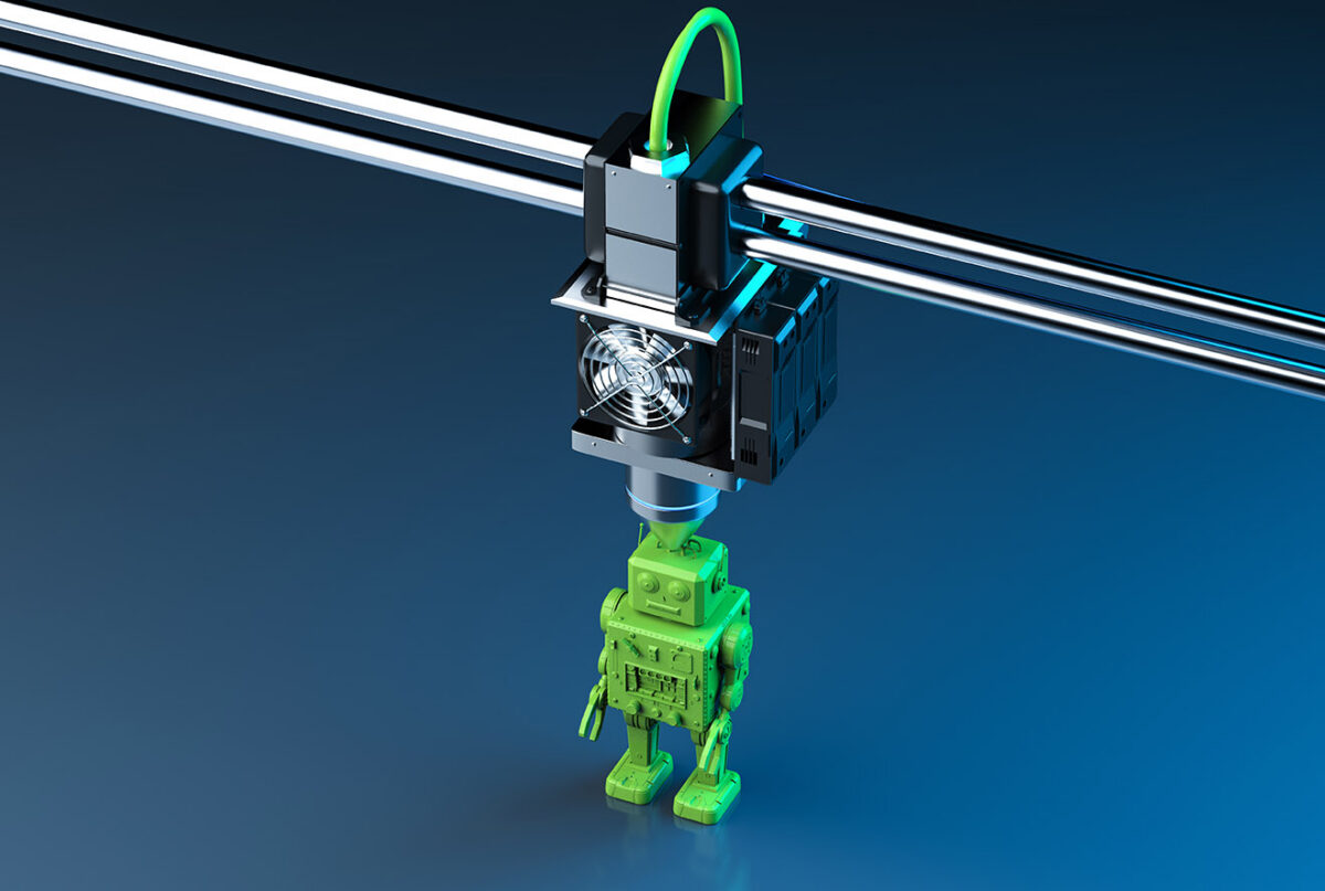
FDM is a common AM approach, but it is also applicable for conductive polymers. This technique uses layers of molten polymers to construct a three-dimensional (3D) object. When creating conductive polymers, manufacturers must use a conductive filament, infused with particles like carbon nanotubes (CNTs), graphene, or metals. With FDM, it is critical to consider part strength and dimensional correctness, as well as the choice of conductive polymer. Print settings can also have a significant effect on FDM parts. FDM is ideal for complex geometry prototypes and products with a short production cycle.
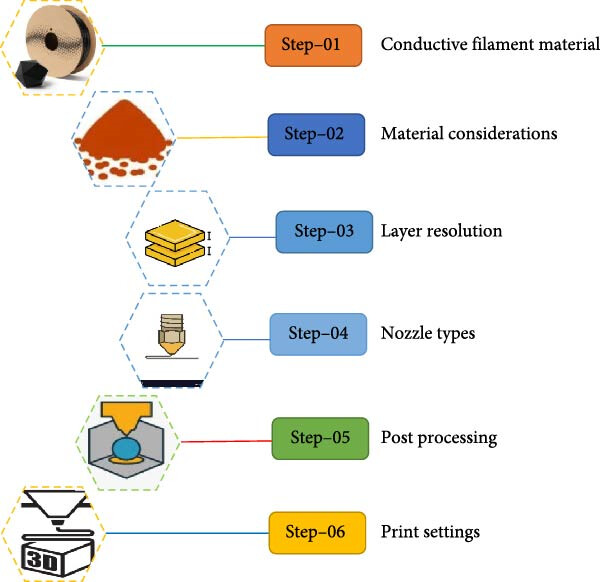
Each step in the FDM process can affect the product output. Figure courtesy of Conductive Polymer-Based Electronics in Additive Manufacturing: Materials, Processing, and Applications.
Stereolithography (SLA)
SLA uses ultraviolet (UV) radiation to cure liquid photopolymer resin to manufacture 3D objects. This method is ideal for complex, high resolution conductive structures. This process involves post-curing, which both ensures the resin completely cures and increases the conductivity of printed parts. SLA is idea for electronic components and prototyping.
Selective Laser Sintering (SLS)
The SLS process uses a powerful laser to fuse layers of powdered polymers. The layers build up to eventually create the 3D object. This method is emerging as a potential approach for producing conductive polymers. Polypyrrole (PPy) is a material of interest for this AM method.
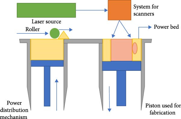
SLS uses a laser to recrystallize powdered polymers. Figure courtesy of Conductive Polymer-Based Electronics in Additive Manufacturing: Materials, Processing, and Applications.
Inkjet Printing
Inkjet printing is an AM process that applies a thin layer of ink to manufacture a 3D object. This method is ideal for a variety of flexible, human-friendly applications, such as wearable electronics. Inkjet printing provides low costs, excellent quality, and high productivity during manufacturing. Droplet-based inkjet printing allows for precise control of ink droplet size, allowing for printing of exact patterns. Solvents, polymers, and metal nanoparticles make up conductive inks for inkjet printing.
You can also read: From Polymers to Patients: Plastics in Wearable Tech.
Cutting Edge Conductive Polymers
Conductive polymers are a source of innovation in the electronic device industry. AM offers an inexpensive, quick method to research and develop these materials and parts. Further avenues of research include the enhancement of conductivity, increasing environmental sustainability, and improving biocompatibility.