3D Printing Shows Potential for Multipart Electronics
Arburg process converts regular pellets and granules into high-tech connected housings
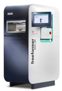
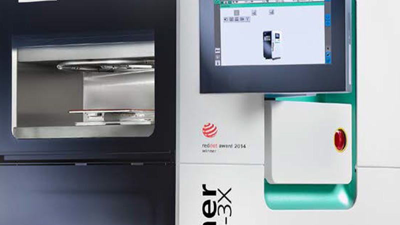
Arburg and Fraunhofer IPA ran 3D-printed
sensor trials on the Freeformer 200-3X unit,
which processes conventional pellets and
granules. Courtesy of Arburg
Injection machine manufacturer Arburg of Lossburg, Germany, recently completed a joint development project with the Fraunhofer Institute for Manufacturing Engineering and Automation IPA, Stuttgart, Germany, and sensor specialist Balluff GmbH, Neuhausen, Germany. The project team used Arburg’s Freeformer 3D printing system and the Arburg Plastics Freeforming (APF) process to create one-of-a-kind electronic position sensors for applications requiring unique shapes.
The “Electronic Function Integration in Additively Manufactured Components” research project ran for 18 months. Stefan Pfeffer, project leader at Fraunhofer IPA, is working with Arburg on research into how conductive plastics can be used in the future to tap additional application areas.
One example of the type of application that was studied in the project is the production of robotic end-of-arm tooling, which often requires position sensors that are almost always specialized in their design, since off-the-shelf sensors may not fit properly. The APF process could also be an important way of producing electronic component housings whose shape and aesthetics are designed for integration and compatibility with innovative platforms in diverse applications.
3D printing, of course, is an attractive option because it allows production of complex shapes that would be difficult—even impossible—to make with conventional forming processes. It also enables the cost-effective production of low-volume batches. One limitation, though, is that not all polymers are available in the filament form required by most standard 3D printers. The APF process operates differently and without this limitation.
The Freeformer processes the same pellets or granulate used in injection molding, so printing application possibilities are greater. The material is processed by a plasticating screw, as in injection molding or extrusion. A nozzle rapidly discharges polymer droplets, which are precisely positioned with the aid of a movable part carrier, and parts are built layer by layer.
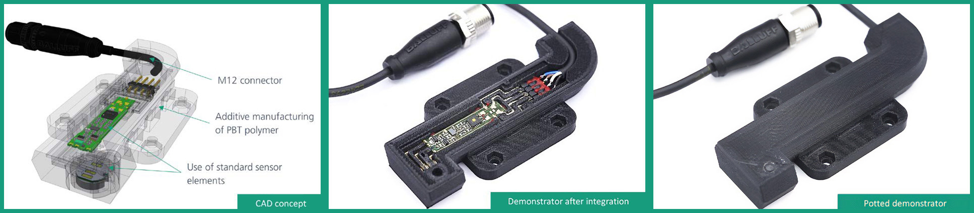
Demonstration model of printed sensor at different production stages: CAD concept (top); after integration of the electronic components (middle); and as a finished demonstrator (bottom). Courtesy of Fraunhofer IPA
Fraunhofer IPA has two Freeformers in its lab. A Freeformer 200-3X model was used in the sensors trials. A semi-crystalline polybutylene terephthalate resin was specified for the high dielectric strength and flame-retardant properties required in the sensor casings. This material is not typically available for filament-based printing. As the layers are deposited, the APF process is automatically interrupted so that the coil, circuit board and plug of the sensor can be integrated. In a separate process, a dispenser is used to produce the silver conductor tracks inside the casing. To complete the process, all that was needed was to overprint the cavities and pot them in polyurethane.
The team produced more than 30 custom sensor units this way and put them through various tests: among them, components had to withstand temperature changes and vibrations, be waterproof and demonstrate electrical insulation. By developing ways to optimize the design and manufacturing process, the tests were ultimately completed successfully.
A possible application, in fact, was discussed with a potential customer at the additive manufacturing trade show Formnext 2021 in Frankfurt last November. The undisclosed manufacturer injection molds housings for electronic components. Two halves of a housing are molded and then glued together after electronics are inserted. The process, however, is not consistent. The company is considering using the APF process wherein half the housing would be 3D-printed first, with electronics inserted next, and the other half then seamlessly printed to complete the unit.
This article was reviewed and edited by Plastics Engineering. For more information on the printer and process, contact Arburg, Lossburg, Germany: +49 7446 33-0; www.arburg.com (U.S. office is in Rocky Hill, Conn. +860-667-6500; www.arburg.us